
Mastering Careers & Skills
Semiconductor Manufacturing: Mastering the Craft · free sample from the book itself
Feras Alzubi
2026 Edition
© 2026 Feras Alzubi. All rights reserved.
No part of this book may be reproduced, stored in a retrieval system, or transmitted in any form or by any means — electronic, mechanical, photocopying, recording, or otherwise — without the prior written permission of the author, except for brief quotations in a review or other fair use permitted by law.
Originality statement. This book is an original work written for this publication. Its text, explanations, worked examples, exercises, skills checks, and case material were created fresh from the field's primary and authoritative sources. No part of this book is copied, recalled, or adapted from any other book, course, or question bank.
Not-affiliated disclosure. This book is an independent study guide. It is not affiliated with, endorsed by, sponsored by, or approved by SEMI, the International Organization for Standardization (ISO), the U.S. Occupational Safety and Health Administration (OSHA), or any employer, school, or training provider. SEMI, ISO, and OSHA are named in this book only as the publishers of standards and rules that technicians work under; naming them does not imply any relationship between them and this book or its author. No government license and no single national certification is required to work as a semiconductor manufacturing technician, and this book confers no license, certificate, credential, or qualification of any kind. It promises readiness and knowledge only.
This book teaches the whole semiconductor manufacturing field from zero to advanced practice, in the order the field itself depends on. Read it in order the first time. Part I builds the foundations — the fab and the field, the honest entry path, the wafer itself, the cleanroom, safety, and the numbers every later chapter uses. Part II walks the process flow in the order a wafer lives it. Part III covers the equipment and fab systems underneath the process. Part IV covers metrology, statistical process control, yield, and quality systems. Part V covers production operations and advanced practice, and ends where this book's field ends: at wafer sort and the hand-off toward packaging, which is another workplace and is signposted, not taught, here.
Every technical term is bolded and defined where it first appears. A term is defined once, at its first use; later chapters use it without re-defining it. Each chapter ends with a Key Terms list collecting that chapter's new terms in one-line definitions, and the glossary at the back of the book is compiled from those lists.
Each chapter follows the same rhythm: a plain opening, why the subject exists, the full working detail, a worked example or realistic scenario, and then a check. The check is the chapter's Exercises & Skills Checks — 15 items in every chapter, with a separate key file in this manuscript and a key section in the finished book that explains the correct answer and why each wrong option is wrong. Calculation items are worked step by step in the key. Do the exercises before you read the key; a wrong answer you have reasoned about teaches more than a right answer you have guessed.
The book also carries a 50-item diagnostic, divided into five strands of ten items each — Cleanroom & Safety, Process Flow, Equipment & Systems, Metrology & Data, and Operations & Judgment — with a strand tracker so you can see which part of the field needs your next study hour. Two batteries of guided process case files and eight strand repair sets complete the practice apparatus. There is no licensing or certification exam for this occupation for the apparatus to imitate, and the book does not pretend otherwise: the apparatus is this book's own design, built to exam-layer depth so that finishing it means you have tested yourself against the whole field, strand by strand.
A note on hands. Semiconductor work is hands-on work, and hands-on qualification happens in an employer's own training and qualification program, on that employer's equipment, under that employer's procedures. This book teaches method, judgment, recognition, and reasoning — how a process works, what a good reading looks like, how to reason from a symptom to a cause, and when to stop and escalate. It does not teach step-by-step performance of hazardous procedures, and where a topic touches hands it says plainly that the employer's program is the gate. That is not a gap in the book. It is the honest shape of the field.
A note on numbers. Process values that vary by tool and recipe — temperatures, pressures, flows, times — are taught in this book as method and as ranges with reasons, never as one tool's recipe. Where a worked example needs a specific number, the example states that number as its own given. The values that do not vary — unit conversions, the standard's own cleanroom limits, the field's standard frequencies and dimensions — are printed exactly, with their source named.
Finally, a note on safety. Chapter 5 is not a chapter to skim. The fab's hazards are real, they are governed by rules that bind, and the technician's part is recognition, compliance, and response — never improvisation and never heroics. Read Chapter 5 before you need it, and return to it whenever a later chapter names a hazard family.
The figures on this page are the only pay and employment figures this book prints. They describe the whole occupation of semiconductor processing technicians — everyone in the occupation, at every level of experience, in every region and every kind of employer — and they are printed exactly as their source states them, with the source named on the face of the page. A median is the middle of the whole occupation. It is not a starting wage, not an offer, not a promise about any one reader, and not a figure for any one employer or any one state.
(Source: U.S. Bureau of Labor Statistics, Occupational Outlook Handbook, "Semiconductor Processing Technicians" (SOC 51-9141), read 2026-11-08.)
Read the entry lines as carefully as the pay line. The occupation's typical entry education is a high school diploma or equivalent, and the training that makes a new hire into a technician is moderate-term on-the-job training provided by the employer. That pairing — modest formal entry education, substantial employer training — is the real shape of the door into this field, and Chapter 2 teaches it whole: the roles employers hire into, the kinds of employers who hire, what voluntary certificates do and do not do, and why no license and no national certification stands in the doorway. In its verified form: the U.S. Bureau of Labor Statistics lists no license for this occupation, and national occupation profiles list no certification requirement. One voluntary credential exists in verified form and is named exactly in Chapter 2 — the SEMI Foundation's SEMI Equipment Maintenance Technician Certification — named there as voluntary and forming, never as a requirement or a hiring gate.
Front matter — Title page · Copyright page · How to Use This Book · The Occupation at a Glance · Contents
Diagnostic — 50 items in five strands of ten, with a strand readiness tracker and key
Part I — Foundations of the Fab — Chapter 1: The Field and the Fab · Chapter 2: Entering the Field: Roles, Employers, and the Honest Credential Landscape · Chapter 3: The Wafer: Silicon, Crystal, and Wafer Making · Chapter 4: Cleanrooms and Contamination Control · Chapter 5: Safety in the Fab · Chapter 6: Numbers of the Fab: Units, Pressure, Vacuum, and Measurement
Part II — The Process Flow — Chapter 7: The Process Flow, Whole · Chapter 8: Photolithography I: Resist and Coat · Chapter 9: Photolithography II: Exposure, Develop, Overlay, CD · Chapter 10: Etch I: Wet Etch and Wafer Cleans · Chapter 11: Etch II: Plasma and Reactive-Ion Etch · Chapter 12: Deposition I: CVD and Epitaxy · Chapter 13: Deposition II: PVD, ALD, and Electroplate · Chapter 14: Thermal Processes: Oxidation and Diffusion · Chapter 15: Ion Implantation · Chapter 16: CMP and Planarization
Part III — Equipment and Fab Systems — Chapter 17: Vacuum Systems · Chapter 18: RF and Plasma Generation · Chapter 19: Specialty Gases and Gas Delivery · Chapter 20: Chemicals and Ultrapure Water · Chapter 21: Components: Valves, MFCs, Sensors, Robots · Chapter 22: Maintenance Method: PM, Troubleshooting, Return to Service
Part IV — Metrology, Yield, and Quality — Chapter 23: Metrology I: Dimensions, Films, Overlay · Chapter 24: Metrology II: Particles, Defects, Inspection · Chapter 25: Statistical Process Control · Chapter 26: Yield: How Dies Are Won and Lost · Chapter 27: Quality Systems: Documentation, Change Control, Audits
Part V — Operations and Advanced Practice — Chapter 28: Running Production: MES, Lots, Dispatch, WIP · Chapter 29: Equipment Qualification and Process Transfer · Chapter 30: Failure Modes and Fab Case Studies · Chapter 31: Advanced Nodes and EUV · Chapter 32: Test, Sort, and the Road to Packaging · Chapter 33: The Technician's Judgment · Chapter 34: Growing in the Field
Every chapter closes with 15 Exercises & Skills Checks and a Key Terms list; every chapter's key explains the correct answer and why each wrong option is wrong (510 chapter items).
Back matter — Process Case Battery A (25 guided case files) with key · Process Case Battery B (25 guided case files) with key · Strand Repair Sets (8 × 15 = 120 items) with key · Study Plans (2-week intensive / 4-week standard) · Cheat Sheets · Figure Program (38 figures — 25 photorealistic plates, 13 diagrams) · Errata & Edition Notes · References · Coverage Crosswalk · Glossary (408 entries)
A modern car will not start, a hospital monitor will not read, and a phone will not wake without parts none of their owners ever see: small squares of patterned silicon, each carrying millions to billions of switches, sealed inside a package and soldered to a board. Those squares were not mined, stamped, or moulded. They were built, layer by layer, on a round slice of silicon in one of the cleanest, most tightly controlled workplaces on earth. This book teaches that building — the whole field of semiconductor manufacturing, from the first definition to the judgment a senior technician exercises on a night shift.
Begin with the plainest definitions the book will offer. A semiconductor is a material whose electrical conductivity sits between a conductor's and an insulator's and can be deliberately changed — silicon is the field's working semiconductor. A semiconductor device is a finished working structure built in and on such a material: a transistor, a diode, or an entire integrated circuit. An integrated circuit (IC) is a complete electronic circuit — many devices and their connections — formed as one patterned structure on a single piece of semiconductor. The place that builds them is a fabrication plant, shortened everywhere in the field to fab: the factory in which wafers are processed into finished circuits. The people this book trains are semiconductor manufacturing technicians — the workers who operate, monitor, maintain, and help qualify the equipment and processes inside a fab. (Source: BLS, Occupational Outlook Handbook, "Semiconductor Processing Technicians" — the occupation covers workers who perform chemical and other processing steps in manufacturing semiconductors.)
Hold the scale honestly from the first page. The features patterned on a modern wafer are measured in nanometres — billionths of a metre — far below what any eye can see and below what ordinary cleanliness can protect. Almost everything strange about a fab — the sealed suits, the filtered air, the vacuum chambers, the obsessive measurement — follows from that one fact: the product is smaller than the dirt. Chapter 4 turns that sentence into a discipline; this chapter builds the map the discipline serves.
The fab's raw material and its finished product are the same object at two moments. A wafer is a thin, round slice of single-crystal semiconductor — today most commonly 300 millimetres in diameter — whose polished surface will carry the circuits. Chapter 3 teaches how a wafer is grown and made; for now, picture a mirror-flat disc, fragile, valuable, and chemically almost perfectly pure.
On that disc the fab prints the same circuit pattern over and over, in a grid, like one photograph tiled across a sheet. Each single repeat of the pattern, once it is finished and separated, is a die — one individual circuit, still unpackaged. A 300 mm wafer carries hundreds to thousands of dies, depending on the die's size: small simple dies number in the thousands, large processors in the hundreds or fewer. A device, in the customer's hands, is what a die becomes after it is tested, separated, mounted, wired, and sealed in its protective package — the black-bodied component a board assembler can handle and solder. This book's field ends at the fab's door: at wafer sort and hand-off awareness (Chapter 32), because assembly and packaging are another workplace with its own craft.
Between the blank wafer and the finished wafer lies the whole book. The wafer does not pass through the fab once, the way a part passes down an assembly line. It loops. A layer of material is deposited; a pattern is printed into a light-sensitive coating; the pattern is etched into the layer; the result is measured; and then the loop begins again for the next layer — dozens of times, building the circuit upward the way a city is built storey on storey, except that every storey must align with the ones beneath it to within nanometres. Figure 1.1 is that loop drawn as a map, and you will return to it in every part of this book.
Figure 1.1 (Class A) — The process-flow loop map: a wafer enters at wafer start, circles repeatedly through deposition, lithography, etch, and measurement — with thermal, implant, and planarization steps joining the loop at their layers — and leaves as a finished wafer bound for sort.
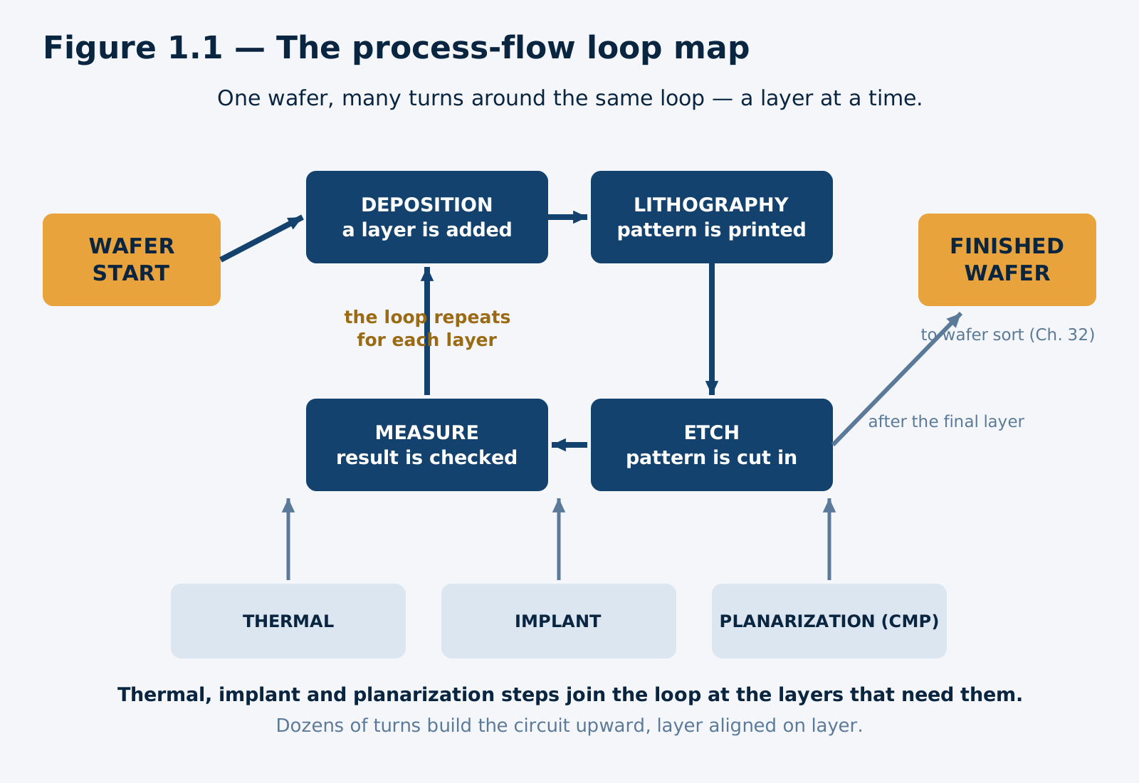
Figure 1.1 — The process-flow loop map: a wafer enters at wafer start, circles repeatedly through deposition, lithography, etch, and measurement — with thermal, implant, and planarization steps joining the loop at their layers — and leaves as a finished wafer bound for sort.
Two consequences of the loop shape govern a technician's whole working life. First, time: because the loop repeats so many times, a single wafer's journey through a fab takes weeks, not hours — the wafer spends most of that time waiting its turn, which is why Chapter 28's production discipline is a real craft and not paperwork. Second, consequence: a defect introduced at layer three is buried under layers four through forty and discovered, if it is discovered cheaply at all, only by measurement at the step where it happened. That is why measurement — metrology, the science and practice of measurement — is not a department at the end of the line but a station inside every loop. Chapter 23 begins its two chapters; its habit begins here: in a fab, you do not assume a step worked. You measure that it worked.
Every step in the loop belongs to one of six families. Learn their names and their one-line jobs now; Part II gives each family its chapters.
Photolithography is the printing family: it transfers a pattern from a template into a light-sensitive coating on the wafer, defining where the next operation will act. It is the loop's pattern-maker, repeated at every layer, and the family's name is shortened everywhere to litho. Etch is the removal family: it takes material away — through the openings litho defined — either with liquid chemistry (wet etch) or with an energized gas (plasma etch). Deposition is the adding family: it lays down a thin, uniform layer — a thin film — of a new material across the wafer, by chemical reaction from gases, by physical vapour, or by related methods. Thermal processing is the heat family: it grows a layer by reacting the wafer's own surface at high temperature, drives atoms into the surface, or repairs and activates what other steps have done. Ion implantation, usually shortened to implant, is the doping family: it fires a controlled beam of atoms, as charged particles, into the wafer to change the electrical behaviour of chosen regions. Chemical-mechanical planarization (CMP) is the flattening family: it polishes each built-up layer back to flatness, because lithography can only print sharply on a flat surface, so every storey must be levelled before the next is printed.
Around those six stands a seventh activity that is not a family but a condition of all of them: cleans — the washing steps, mostly wet-chemical, that strip particles and residues from the wafer between operations. A wafer is cleaned far more often than it is patterned; contamination is the field's standing enemy, and cleans are its standing answer, taught with wet etch in Chapter 10 because they share its benches and its chemistry discipline.
No family is the glamorous one and the others support. A fab is a chain of loops in which every family is, in turn, the step the whole wafer is waiting for. The technician who understands only one family's tools can run a station; the technician this book aims at understands the loop, and can therefore reason — when a measurement drifts, when a lot waits, when a chamber misbehaves — about what the wafer needs next and what a fault here will cost three loops from now.
The loop also explains the fab's strange relationship with failure. In an assembly plant, a bad part is one bad part. In a fab, a bad step can quietly spoil every wafer that passed through it during the hours before a measurement caught it — which is why lots are tracked so that every wafer's complete step history can be reconstructed, why tools hold production when their monitors fail rather than letting product "probably fine" flow onward, and why the hold is respected by every role without argument. Traceability is the fab's insurance policy: when a defect is finally understood, the record says exactly which wafers shared the suspect step, and the loss is bounded to them instead of spreading by suspicion across weeks of output. A technician experiences this system as paperwork — lot travellers, tool logs, hold tags — and should understand it as the difference between an incident and a catastrophe. The record is not bureaucracy laid over the work. In a workplace where the product cannot be inspected by eye and the process cannot be watched directly, the record is the work's visible form, and every later chapter's discipline — qualification, change control, SPC, yield analysis — is built on its accuracy.
A fab's production floor is organized for one master purpose: nothing unfiltered touches the wafer's world. The processing area is a cleanroom — a room whose air is continuously filtered and whose particle count is held to a classified limit — and Chapter 4 teaches its classes and discipline whole. Within it, the floor is laid out in bays: aisles flanked by rows of equipment, arranged so wafers travel short, ordered paths between the tools of successive steps, and so that the dirtiest necessary work happens farthest from the most sensitive steps.
The equipment itself is called, in the field's universal shorthand, tools — not hand tools, but entire machines, many the size of a wardrobe or a small room: a lithography scanner, an etch chamber system, a deposition furnace, an implanter, a polisher, a measurement station. A single tool may contain vacuum chambers, gas and chemical delivery, robotics, computers, and its own internal clean environment cleaner than the room around it. Part III teaches the systems those tools are built from; Part II teaches what each family of tools does to the wafer.
Wafers almost never travel naked or one at a time. Production wafers move in lots — a tracked group of wafers, commonly up to twenty-five, that travel together through the flow as one unit of work — carried in a sealed pod. For 300 mm production that pod is a FOUP (front-opening unified pod): a lidded plastic carrier that holds the lot in its own filtered micro-environment and opens only when docked to a tool's load port, so the room's air never reaches the wafers at all. Automated rails and vehicles move FOUPs between bays overhead; at the tool, a robot unloads wafers one at a time into the process and returns them when the step is done. Chapter 21 teaches the handling machinery; the habit to form now is that a wafer is handled by its carrier and by robots, in a sealed chain, from wafer start to sort — every break in that chain is a contamination event, and the field treats it as one.
Around the cleanroom stands the fab's other half, which a new technician must respect equally: the subfab and support areas below and beside the floor, where pumps, abatement units, chemical and gas delivery, ultrapure water, power, and exhaust live and where much equipment-technician work is done; and the gowning areas where every person entering dresses in the cleanroom ensemble that makes a human — the fab's largest particle source — safe to stand beside a wafer. Facilities technicians keep those support systems alive; Chapter 2 separates the technician roles properly.
Four technician roles recur through this book, named here in outline and taught whole in Chapter 2. Process technicians support the recipe side: they monitor process results, run qualification and monitor wafers, and work with engineers on whether a process is behaving. Equipment technicians keep the tools themselves alive: preventive maintenance, troubleshooting, repair, and the disciplined return of a tool to service. Manufacturing technicians — the operators of the flow in many fabs — move lots, run tools to their procedures, watch the production queue, and are the loop's daily hands. Facilities technicians maintain the plant systems the cleanroom breathes through: water, gases, chemicals, vacuum support, power, and exhaust. The boundaries differ by employer, and one person may wear two of these hats in a small fab; what does not differ is the shared ground — cleanroom discipline, safety rules, measurement honesty, and written records — that this book teaches as one craft.
Above and beside the technicians stand engineers, supervisors, and quality and yield specialists, and a technician's craft includes working with all of them: escalating with evidence, writing records another shift can act on, and knowing which decisions are a technician's to make and which are not. Chapter 33 is devoted to that judgment. For Chapter 1, hold the simpler truth: nobody in a fab works alone on a wafer. A lot that a manufacturing technician runs at noon is measured by a process technician at two, on a tool an equipment technician returned to service at nine, in a room a facilities technician's systems kept in class all night. The fab is a relay, and the baton is information.
See the roles at work on a single ordinary problem, because the relay is easier to learn in motion than in a list. A deposition tool's film-thickness measurements begin drifting upward across a morning — not out of limits, but moving, the way Chapter 4's particle trend moved. The process technician who spots the trend does not adjust the recipe: recipe changes are governed changes, made with engineering authority and recorded under Chapter 27's discipline. Instead she gathers the evidence properly — the monitor data, the timing against the tool's last maintenance, the lots processed since — and raises it with the tool's equipment technician and the process engineer. The equipment technician's checks find a sensor drifting in its own right: the tool was telling the truth about a measurement that was lying. The fix is a sensor replacement under maintenance procedure, a monitor run to prove the tool again, and a documented release — and the manufacturing technicians, whose lots waited through the hold, restart the queue in dispatch order with the held lots' positions explained rather than assumed. Four roles touched one drift; none of them could have closed it alone; and the wafer lots at stake never knew how close they came to being built on a lying number. That is the fab working as designed, and it is why this book teaches all four roles to every reader regardless of the one they will first be hired into: you cannot hand a baton cleanly to a runner whose job you do not understand.
The same scene teaches the fab's information ethic in miniature. At no point did anyone round a reading, backdate a record, or release the tool on a verbal assurance — not because a rule was watching, but because every person in the chain knew the next person's decision would be built on their record. A fab's records are load-bearing. Engineers design changes on them, quality systems certify product on them, and customers accept or reject shipments on the strength of the data package the records become. Chapter 27 formalizes the system; Chapter 1 asks only that you feel the weight now: in a fab, writing it down is doing it, and writing it down wrong is doing it wrong, however skilled the hands that did the physical work.
Fabs run continuously. A production fab does not close at night, because tools that cost what these tools cost and processes that take weeks cannot pause for weekends; the plant runs twenty-four hours, in shifts — commonly twelve-hour rotating shifts, arranged so each crew works blocks of days and nights with blocks off between. Chapter 2 discusses shift life honestly as part of the real job; here, see what the continuity means for the work itself.
A shift begins with handover: the outgoing crew passes the incoming crew the state of the plant — which tools are running, which are down and why, which lots are urgent, which measurements are drifting, what to watch. Handover is a formal, written, disciplined act, because the fab's memory cannot live in one person's head across a twelve-hour gap. Through the shift, work flows from a dispatch queue managed in the fab's computer system (Chapter 28): lots are run in priority order, monitor wafers precede production after any maintenance, tools are measured against their control charts (Chapter 25), and every significant event — a fault, a hold, a repair, a release — is written into the record at the time it happens.
Walk one small scene, a composite of ordinary fab life. At shift start, an etch tool stands released after overnight maintenance. Before any production lot touches it, a monitor wafer runs and its etch result is measured and compared with the tool's control limits: the tool must prove it is back before the fab trusts it with weeks-old product wafers. The measurement is in limits; the release is logged; the first lot docks, its FOUP opens against the load port, and the loop turns again. Nothing in that scene is dramatic, and that is the point: a fab's drama is prevented, shift by shift, by exactly this order — prove, record, then produce. A technician who internalizes that order in Chapter 1 has already learned the field's deepest habit.
Close the map with the standing honesty this book keeps on its face. The U.S. Bureau of Labor Statistics lists no license for this occupation, and national occupation profiles list no certification requirement, to work as a semiconductor manufacturing technician. Employers hire on education, aptitude, and their own training and qualification programs; the occupation's typical entry education is a high school diploma or equivalent, with moderate-term on-the-job training. (Source: BLS, Occupational Outlook Handbook, "Semiconductor Processing Technicians," read 2026-11-08.) Chapter 2 teaches that landscape whole, including what voluntary industry certificates are and are not.
This book therefore promises readiness and knowledge only. It confers no credential, satisfies no employer's training requirement, and guarantees no job or income. What it does do — if you work it whole, exercises included — is give you the field entire: the physics under the processes, the processes in their order, the equipment and its systems, the measurement and yield disciplines, the safety law, and the judgment to know what you do not yet know. In a field whose employers train, the applicant who arrives already speaking the fab's language — loop, lot, class, control limit, hand-off — starts that training far ahead. That is a book's honest promise, and it is enough.
One more picture completes the map, because beginners consistently underestimate both halves of it: how much value a single wafer accumulates, and how long it takes to accumulate it. A finished wafer's dies may become the processors in medical equipment, the controllers in a power grid, or the memory in a vehicle — and the wafer that carries them spent weeks travelling the loop of §1.2, visiting hundreds of individual process steps, each with its own setup, its own measurement, and its own chance to end the wafer's story. At every step the wafer carries all the value of every step before it. A wafer destroyed at step twelve has lost an afternoon; a wafer destroyed at step four hundred has lost weeks of the fab's most expensive hours. That rising value is why the fab's caution rises as a lot ages, why old lots are handled by the most experienced hands, and why the word scrap — a wafer or lot removed from production as unrecoverable — is spoken in a fab with genuine weight.
The same arithmetic explains the fab's economics at the level a technician needs. The building, its air, its water, its gases, and its tools cost the same whether they process one wafer or a thousand, so the fab's health is measured in throughput and in yield together — a tension Chapter 26 teaches formally. It also explains why tools are never casually stopped and why maintenance is scheduled with the same seriousness as production: an idle bottleneck tool is not resting; it is a queue of ageing, value-laden lots growing behind it. A new technician does not need the fab's accounts. They need the instinct those accounts produce in experienced staff: treat every wafer as weeks of other people's work riding in your carrier, because it is.
Finally, place the fab among its neighbours so the map's edges are as clear as its centre. Upstream stand the wafer makers of Chapter 3 and the suppliers of gases, chemicals, and equipment. Downstream stand sort, assembly, packaging, and final test (Chapter 32's signpost), and beyond them the board assemblers and the makers of every electronic product. The fab is the middle of that chain and its most demanding link — the link where a disc of sand-derived crystal becomes, layer by measured layer, the working heart of the modern world. The rest of this book teaches how, family by family and system by system, in the order the wafer lives it.
Close the chapter by walking the map once, slowly, as a single lot lives it. A lot of twenty-five wafers arrives at wafer start in its FOUP, documented, its material identity already verified against the reading Chapter 3 will teach. Nothing about the lot is impressive to look at — a sealed pod, a traveller record, a queue position — and everything about its next weeks is already implied by those three things: what it is, what it must become, and what stands ahead of it in line.
The first loop begins with deposition. The tool's robot takes each wafer in turn, a thin film is laid down across its face, and the wafers return to the pod in order. Before the lot may travel onward, a measurement from that step is read against its limits: not the lot's own product wafers torn down for inspection, but the step's monitor evidence, gathered exactly as §1.5's drift scene described. The film measures inside its band. The record is written — tool, recipe, time, result, operator — and only then does the dispatch system release the lot to lithography, where the coating that will carry this layer's pattern is applied and printed. Etch follows, removing material through the pattern's openings; another measurement closes the loop; and the lot returns to its FOUP carrying one finished storey of its circuit and a record one loop longer.
Notice what the walk keeps showing, because it is the chapter in motion. At no station did anyone hurry the lot past a measurement to save an hour, because an hour saved at loop one is spent a hundredfold when a buried fault surfaces at loop thirty. At no station did the wafer meet room air, a bare hand, or an undocumented decision. And at every station a different member of §1.5's relay held the lot — running it, measuring it, or keeping the room and the tool beneath it in their specified states — and passed it onward with the record as the baton. Multiply that one loop by the dozens the product requires, add the thermal, implant, and planarization steps joining at their layers, and you have the lot's whole biography: weeks of travel, hundreds of steps, thousands of recorded facts, all in service of dies that will not be known good or bad until sort. A technician who has pictured that biography once, whole, reads every later chapter differently — each process, system, and rule that follows exists because some moment in this walk demands it.
Tags: FIELD — the field and the fab; FLOW — the process-flow loop. The key, with every option explained, is in this chapter's key file.
Q1. A fab's finished output, before packaging, is best described as: A. Packaged devices ready to solder to a board B. Individual dies already separated and sealed C. A finished wafer carrying many completed dies, bound for sort D. A blank wafer that has been polished and cleaned
Q2. In this book's vocabulary, a die is: A. A tool used to cut wafers apart on the production floor B. One individual circuit on a wafer, one repeat of the tiled pattern C. The package a finished circuit is sealed inside D. A defective wafer removed from a lot
Q3. Why does a wafer loop through the process families many times instead of passing down a line once? A. Because tools are too slow to finish a layer in one pass B. Because each loop re-polishes damage from the loop before C. Because wafers must wait for cleanroom space to free up D. Because the circuit is built up layer by layer, each layer patterned and processed in turn
Q4. The first and deepest reason a fab is built around filtered air, sealed carriers, and suits is that: A. The features patterned on the wafer are smaller than the dirt that could land on them B. Silicon is poisonous and must be shielded from workers C. The chemicals used are all odourless and must be contained for smell D. Customers require photographs of a spotless factory
Q5. Photolithography's job in the loop is to: A. Define where the next operation will act, by transferring a pattern into a light-sensitive coating B. Remove material from the wafer through openings in a mask C. Lay down a uniform thin film of new material D. Fire a beam of charged atoms into the wafer surface
Q6. Which pairing of family and job is correct? A. Etch — laying down a thin film; Deposition — removing material B. Implant — flattening a layer; CMP — doping a region C. CMP — flattening a built-up layer; Implant — changing a region's electrical behaviour with a beam of atoms D. Thermal — printing a pattern; Litho — growing oxide
Q7. A FOUP's purpose is to: A. Hold finished devices for shipping to customers B. Carry a lot of wafers in a sealed, filtered micro-environment that opens only at a tool's load port C. Store chemicals safely between deliveries D. Cool wafers after high-temperature steps
Q8. Before a tool released from maintenance runs production lots, the fab's order of work is: A. Run the hottest lot first to prove the tool under load B. Skip monitors whenever the repair was minor C. Let the next shift decide whether the tool is ready D. Run a monitor wafer, measure its result against control limits, and log the release
Q9. Metrology's place in the fab is best stated as: A. A final inspection performed only after the last layer B. A department that measures only defective wafers C. Work done only by engineers, never by technicians D. A station inside every loop — a step is not assumed to have worked; it is measured
Q10. Which statement about entering this occupation is true? A. No government license and no single national certification is required; employers hire and train through their own programs B. A single national exam licenses semiconductor technicians in every state C. This book's exercises, once completed, constitute a certification D. A voluntary certificate is a legal requirement for fab employment
Q11. A lot, on the production floor, is: A. A single wafer processed entirely alone B. The parking area where FOUPs wait between bays C. A tracked group of wafers that travel together through the flow as one unit of work D. The total output of one shift
Q12. The four technician roles named in this chapter are: A. Process, equipment, sales, and marketing technicians B. Process, equipment, manufacturing, and facilities technicians C. Chemical, electrical, mechanical, and software technicians D. Junior, senior, lead, and principal technicians
Q13. Handover at shift change matters because: A. It is a legal ceremony with no operational content B. The fab runs continuously, so its memory — tool states, urgent lots, drifting measurements — must pass formally between crews C. Incoming crews are not permitted to read written records D. It replaces the need for any computer production system
Q14. This book's field ends, and another workplace's craft begins, at: A. The design of the circuit itself B. The mining of silicon-bearing sand C. The soldering of packaged devices onto boards in a customer's factory D. Wafer sort and hand-off awareness — assembly and packaging are signposted, not taught
Q15. A thin film is: A. The plastic film that seals a FOUP for transport B. A protective coating applied to finished packages C. A thin, uniform layer of material laid down across the wafer by deposition D. The light-sensitive coating used only in lithography
Semiconductor — a material whose conductivity sits between a conductor's and an insulator's and can be deliberately changed. Semiconductor device — a finished working structure, such as a transistor or an integrated circuit, built in and on semiconductor material. Integrated circuit (IC) — a complete electronic circuit formed as one patterned structure on a single piece of semiconductor. Fab — a fabrication plant: the factory in which wafers are processed into finished circuits. Wafer — a thin, round slice of single-crystal semiconductor whose polished surface carries the circuits. Die — one individual circuit on a wafer; one repeat of the tiled pattern, before separation and packaging. Package — the protective body a tested die is mounted and sealed in, so it can be handled and soldered. Photolithography (litho) — the process family that transfers a pattern into a light-sensitive coating, defining where the next operation acts. Etch — the process family that removes material, by liquid chemistry or by plasma, through openings a pattern defines. Deposition — the process family that lays down a thin, uniform layer of new material across the wafer. Thin film — a thin, uniform layer of material deposited across the wafer. Metrology — the science and practice of measurement; in the fab, a station inside every process loop. Lot — a tracked group of wafers that travel together through the flow as one unit of work. FOUP — front-opening unified pod: the sealed carrier that holds a 300 mm lot in its own filtered micro-environment.
End of the free sample. The complete book continues from here — the full A-to-Z course in book form, delivered as an EPUB you can read in Apple Books, Google Play Books, ReadEra, Thorium Reader, Adobe Digital Editions, or Send to Kindle.
Buy this ebook — $12.99 Back to the book page
Payments are securely processed by Payhip.